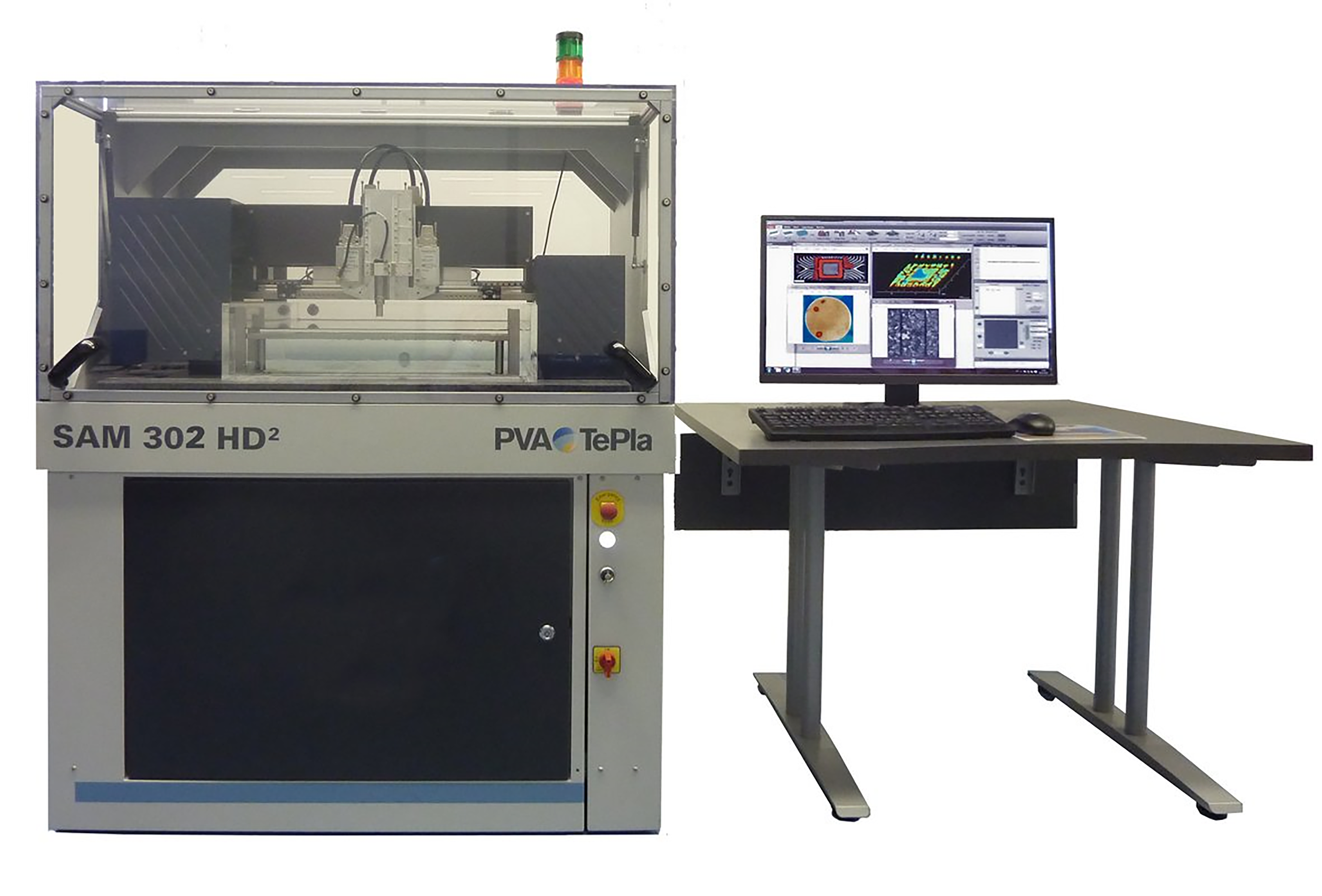
Scanning Acoustic Microscope designed by PVA TePla Analytical System
PVA TePla Analytical Systems designs and manufactures state of the art Scanning Acoustic Microscopes. Technological developments have focused on the detection of structural defects and materials characterization within opaque materials. Voids, inclusions, delaminations, cracks and even density variations are all defects sensitive to the technique of acoustic microscopy.
Why Use Scanning Acoustic Microscopy?
The main feature of Scanning Acoustic Microscope (SAM) is its ability to non-destructively examine the interior of opaque materials with the resolution of an optical light microscope. The demand for non-destructive imaging and materials analysis has increased significantly in recent times. For instance, quality control Inspection and process optimization are paramount for the semiconductor, microelectronics and MEMS industries where SAM technology is now fast becoming the technique of choice. PVA TePla Analytical Systems excels in innovations and developments of advanced solutions applications using Scanning Acoustic Microscopy for both laboratory and production environments.
Proprietary Transducer Technology
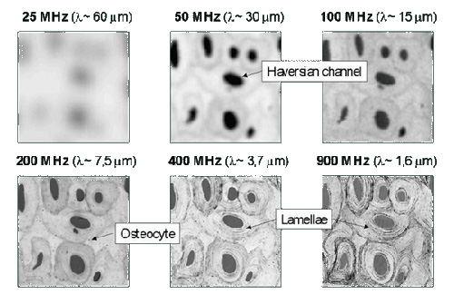
The resolution of SAM is critical to its application and depends heavily on the transducer technology. PVA TePla Analytical Systems designs and manufactures unique transducers using proprietary thin film technology. From this development a new generation of transducers arose with the world’s widest frequencies ranging from 3 to 2000 MHz. As a result PVA TePla is now the global leader in image resolution and analytical capabilities.
Global Service and Support Network
When it comes to after sales and applications support, PVA TePla Analytical System’s has an extensive global network with laboratories in Europe, US and Asia. Our experienced application engineers are dedicated to their profession and and have a deep understanding of our customers needs.
Designed to Scan
In addition to our proprietary transducer technology, PVA TePla Analytical Systems’ scanners are designed to adapt to a broad range of applications:
Ultra fast linear motion scanners with high acceleration allow both high throughput and precise scans.
In-line inspections in production environments are performed by fully integrated automated systems.
Ultra-high resolutions (>1μm) are achieved with our dedicated laboratory systems.
Product Platform Strategy
One of our major success factors is the development of a common platform of shared components upon which we configure hardware according to the customer’s needs. The benefit passed on to our customers include:
High performance / price ratio.
Improved serviceability resulting in affordable cost of ownership.
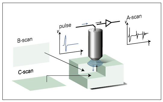
Operation Principle of Scanning Acoustic Microscopy SAM utilizes ultrasound to non-destructively examine internal structures, interfaces and surfaces of a substrate….
FHI Halle, Germany Development partner for quantitative estimation of material parameters using ultra high frequency scanning acoustic microscopy: -Analysis of…
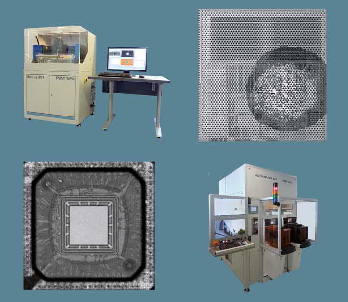
Applications for Semiconductor Industry Scanning Acoustic Microscopes (SAM) are used for non-destructive failure analysis, research and development, quality control, and…
WINSAM 8 PVA PVA TePla Analytical Systems proprietary measurement and analysis software. Visualisation Dedicated non destructive imaging and analysis of…
SAM is a non-destructive technique used to investigate samples like the integrated circuit represented above. For a more complete understanding of acoustic interactions and analytical convenience different scan modes