Surface wettability adjustment
Surface wettability adjustment for ink jet printing of PLEDs.
Surface properties of the ITO electrode and the bank resist structure are critical to both the elec-trical and optical perfor-mance of PLED displays.
Stress Imaging
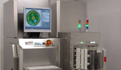
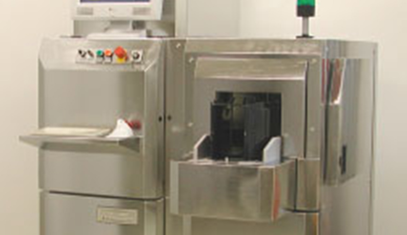
Fast Monitoring of Mechanical Stress on up to 300mm Wafers.
The introduction of 300mm wafers has imposed new, higher standard requirements on suppliers of bare wafers: By increasing diameter from 200 mm to 300mm
Solar Cell Etching
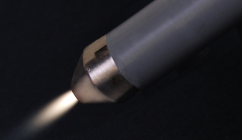
Edge isolation of solar cells by plasma etching. Dry plasma etching for edge isolation of solar cells is a proven and economic solution and widely used in cell fabrication lines.

Photoresist Ashing
Plasma photoresist ashing following etching and ion implantation is one of the most important and frequently performed steps in semiconductor fabrication.
MEMS SU Ashing
SU8-photoresist has many remarkable properties that are ideally suited for use in the fabrication of MEMS and microfluidic devices. Among the many merits of this photoresist for MEMS manufacture, is its chemical stability, which makes it difficult to remove.
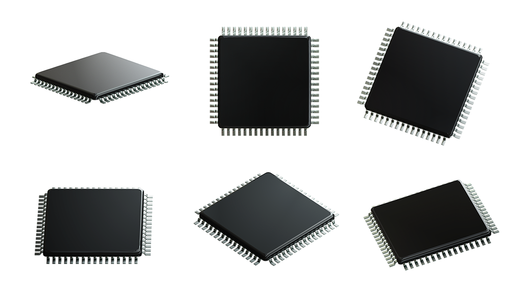
Implant Dosage
The Implant process is a very critical step within the integrated circuits manufacturing line. It defines important characteristics and properties of the devices-to-be by doping certain layers of the silicon substrate.
Flip Chip Underfill
Plasma cleaning in FlipChip packaging technology has become a must for yield improvement. Advanced Flip Chip devices are gaining in market prominence
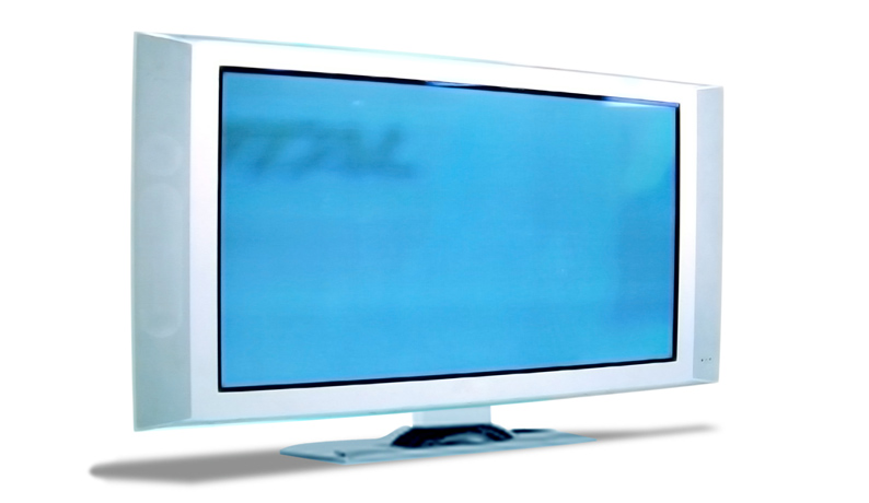
Flat Panel Photoresist Ashing
Uniform Plasma cleaning of large substrates for manufacturing of display requires a scalable system concept. The planar microwave plasma systems are designed for such applications
Encapsulation
In semiconductor micro-chip packaging, microwave plasma cleaning and activation is used in applications of adhesion promotion of encapsulant mold compounds.
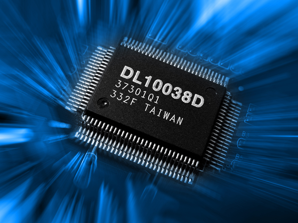
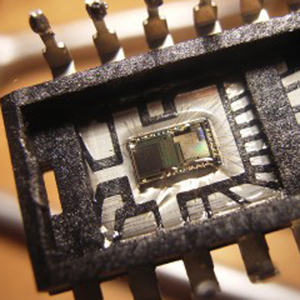
Decapsulation
Decapsulation of packaged devices (such as integrated circuits (IC’s) and printed circuit boards (PCB’s)) exposes the internal components of the package. Opening devices by decapsulation allows inspection of the die, interconnects and other features typically examined during failure analysis.
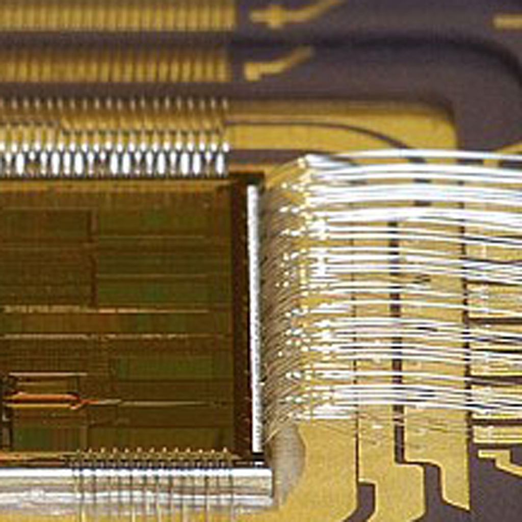
Bond Pad Cleaning
In chip packaging, plasma cleaning is essential for improving the cleanliness of bond pads prior to wirebonding. Ball shear and stitch pull strengths are dramatically enhanced by surface plasma cleaning.
Bond Finger Cleaning
Plasma cleaning can also be applied to the packaging of Flat Panel Displays. For example, LCD or OLED terminal cleaning to remove organic contaminants from the bond fingers prior to connective bonding and conductive film adherence.