PVA TePla / Quality
Each of PVA TePla’s manufacturing sites are ISO 9001:2015 registered and also assembly according to SEMI and European CE-Standards depending on the systems final installation site.
PVA TePla is one of the world’s leading system engineering companies. Its core competencies are in the fields of systems for hard-metal sintering and crystal growing as well as the use of plasma systems for surface activation, functionalization, coating, ultra-fine cleaning and etching.
Each of PVA TePla’s manufacturing sites are ISO 9001:2015 registered and also assembly according to SEMI and European CE-Standards depending on the systems final installation site.


As a result of a management buy-out, Peter Abel GmbH takes over the vacuum metallurgy systems division of what was then Arthur Pfeiffer Vakuumtechnik Wetzlar GmbH (now: Pfeiffer Vacuum Technology AG) and establishes PVA-Pfeiffer Vakuum Anlagenbau GmbH (subsequently: PVA Vakuum Anlagenbau GmbH). The company focuses on the construction of systems for manufacturing and refining materials subjected to high temperature, vacuum, and pressure.
To provide additional production capacities, PVA Vakuum-Anlagenbau Jena GmbH is founded. In addition, a “spin-off” of Leybold Systems leads to the founding of Crystal Growing Systems (CGS) GmbH in Hanau, Germany. The company specializes in the construction of systems for manufacturing monocrystalline silicon crystals for the semiconductor industry.
In the same year, TePla AG is floated with an IPO on the Frankfurt Stock Exchange. TePla AG develops, manufactures, and sells innovative plasma systems for the semiconductor industry as well as measuring systems based on laser technology.
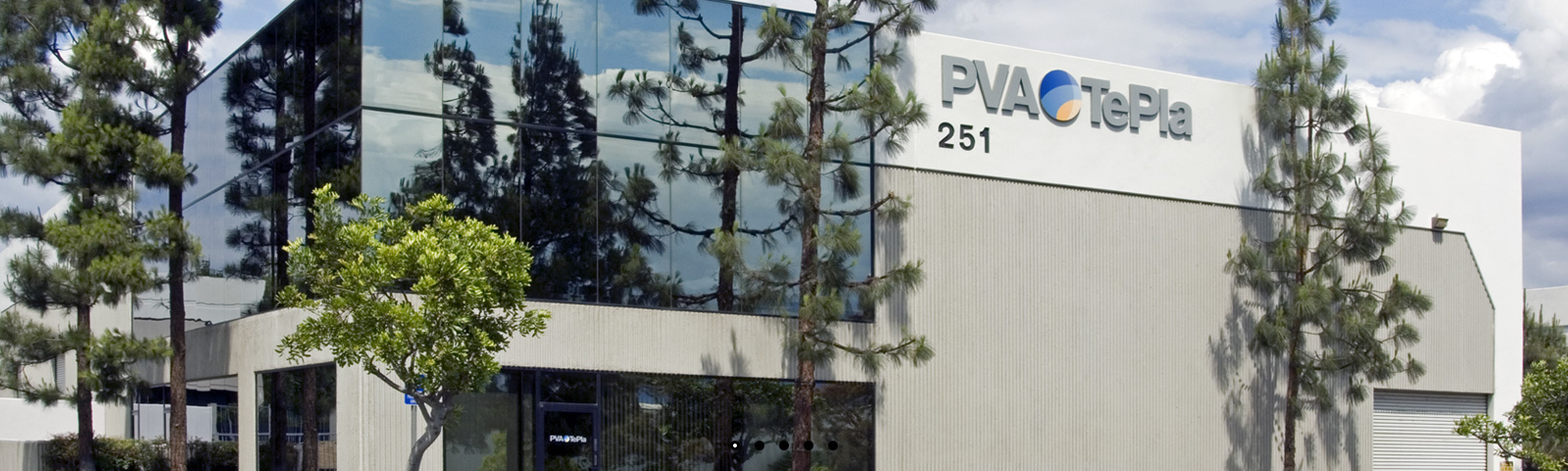
A branch is established in the US under the name of PVA USA Corp. (subsequently PVA TePla America, Inc.).
PVA Vakuum Anlagenbau GmbH and TePla AG merge to become PVA TePla AG with its headquarters in Aßlar (subsequently relocating to Wettenberg).
In the same year, PVA Löt- und Werkstofftechnik GmbH (LWT) is established. It takes over the business area of brazing and heat treatment from the parent company.
In the US, a merger takes place between PVA USA and TePla America to form PVA TePla America Inc. It represents all divisions of PVA TePla AG on the American market and concentrates on the development and construction of plasma systems for the medical/life science area.
Following the takeover of the float-zone crystal growing business area of Danish company Haldor Topsoe, PVA TePla Danmark is founded. The company goes on to become with world’s leading provider of float-zone (FZ) systems.Following the takeover of the float-zone crystal growing business area of Danish company Haldor Topsoe, PVA TePla Danmark is founded. The company goes on to become with world’s leading provider of float-zone (FZ) systems.
PVA TePla establishes Xi´an HuaDe CGS Ltd. in China as a joint venture with the Technical University Xi’an (TUX).
Crystal Growing Systems GmbH relocates from Hanau to Aßlar to the headquarters of the parent company.
PVA TePla (China) Ltd. marks the opening of a service and sales branch in Beijing. The Group now has direct access to the important Chinese market, especially for its high-temperature systems.
After acquiring the business of Plasma Technik Grün GmbH in Siegen, PVA TePla AG, trading as PlaTeG GmbH, opens a new division—Vacuum & Nitriding Systems—that focuses on manufacturing systems for the plasma nitriding of surfaces.
Following the takeover of Krämer Scientific Instruments GmbH in Herborn and its Aalen-based subsidiary SAM TEC GmbH, PVA TePla enters yet another new field: ultrasonic microscopy. Both companies are renamed in 2008 to become PVA TePla Analytical Systems GmbH. The company headquarters are initially in Aalen and currently in Westhausen.
PVA TePla AG leaves its previous headquarters and its production facilities for vacuum systems in Aßlar and relocates to the town of Wettenberg near Giessen.
The company divisions are reorganized and are now called: Industrial Systems, Semiconductor Systems, and Solar Systems.
PVA TePla acquires Munich Metrology GmbH in Munich, thereby strengthening the technological expertise of PVA TePla in the area of metrology. Munich Metrology—subsequently incorporated into PVA Metrology & Plasma Systems GmbH—concentrates on the detection of metallic contaminants on wafer surfaces in the semiconductor industry.
JenaWave GmbH—which has also since merged to become part of PVA Metrology & Plasma Systems GmbH—is acquired by PVA TePla. By developing and constructing what are considered to be the key components of optical measuring heads, including complex evaluation and control software for the analysis systems, PVA TePla AG further bolsters its metrology division.
The reorganization of the corporate group with PVA TePla AG as a holding company and the subsidiaries as operating units establishes a more flexible and efficient organizational structure.
In 2016, PVA TePla further strengthened its position in the Chinese market by establishing a further sales and service location in the Xi’an high-tech region.
With a new design and clear structuring of the divisions, the status of PVA TePla as a strong group of companies is now further emphasized.
PVA SPA Software Entwicklungs GmbH is a specialist for software and automation in the semiconductor industry as well as for optical metrology. This acquisition represents an important step forward for the further strategic development of the PVA TePla Group.
In 2019, the PVA TePla Group took over the activities of a renowned and globally acknowledged Italian vessel. As a result, our subsidiaries will be able – in addition to our existing suppliers – to purchase vessels from own production for the manufacturing of vacuum and crystal growing systems.