Teflon Activation
Teflon® ( Polytetrafluoroethylene ) , with its very low dielectric constant, is an excellent material to ensure fast signal propagation and superb isolation properties.
Stamper Conditioning
Poor polycarbonate release properties after stamping can scratch and snag the data bits during detachment of the replicate from the…
Stamper cleaning
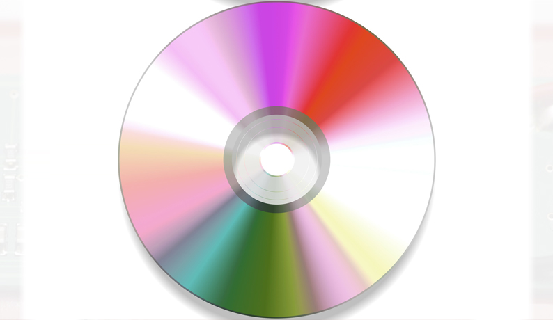
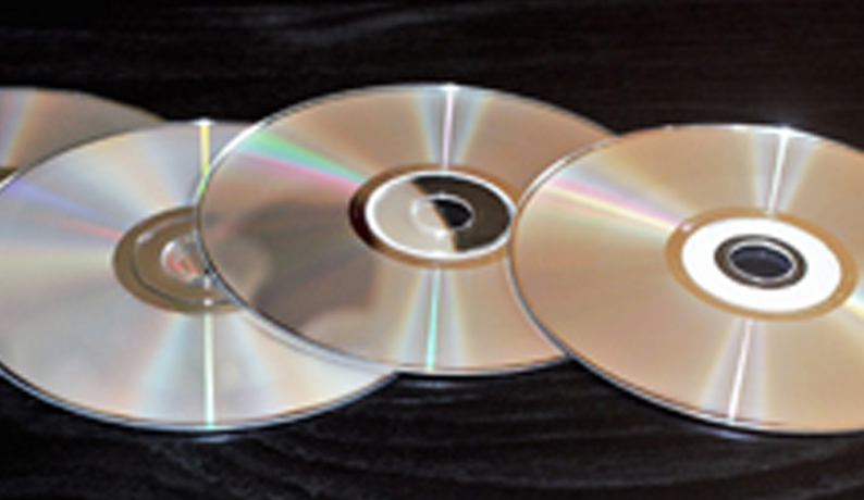
With the advent of Blu-ray formats, optical disc technology celebrates its third generation of high density data storage media. As…
Potting
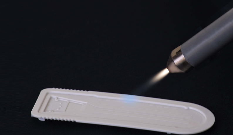
Plasma activation prior to potting ensures a good hermetic seal, reduces current leakage and provides stronger physical bonding to the device. The protection of electronic or electrical devices
Feedthrough potting
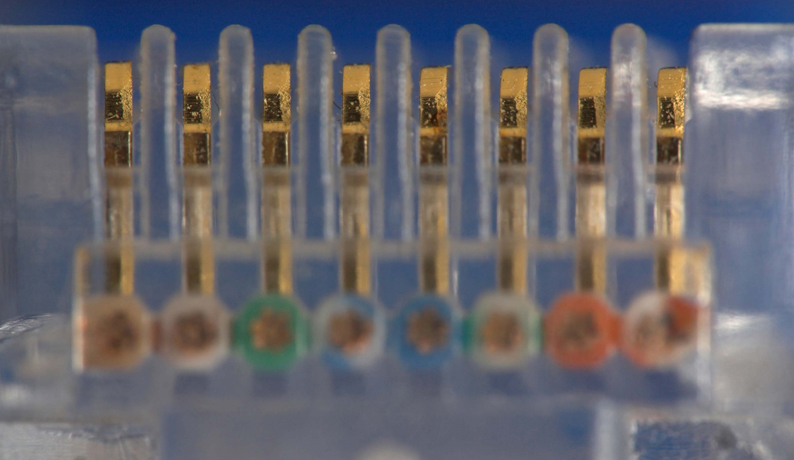
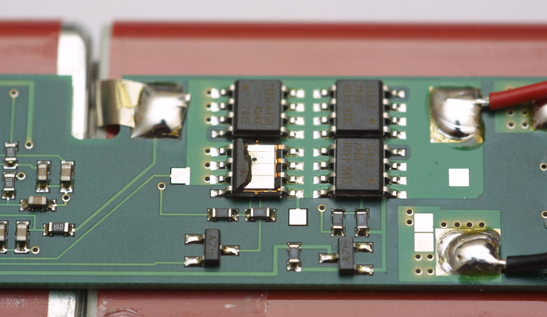
Electronic connectors and cable assemblies are used for communications and data transfer applications as well as for power connections. The…
Desmear
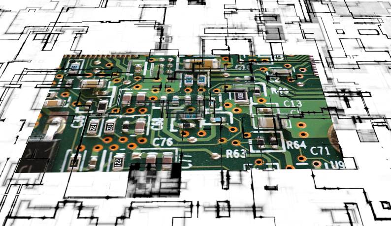
Plasma desmear and etch-back by plasma is an established practice in the PCB industry. Drilling vias through multilayer PCB’s leaves residue, or smear, on the via walls.
Anisotropic conductive film
Plasma is used to promote the adhesion of anisotropic conductive film in flat panel display manufacture An LDI chip is…
Carbon Ash
Metallization of through-vias is often impeded by carbonaceous deposits formed during laser drilling. To remove these deposits from vias, the printed circuit boards are immersed into gas plasma
Adhesion promotion
Improve adhesive bond properties of materials. Plasma is ideal for treating plastics, metals, ceramics, and glass prior to adhesive bonding. In each case, loose boundary…