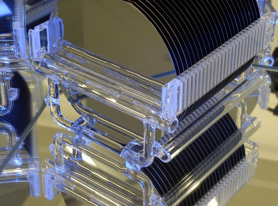
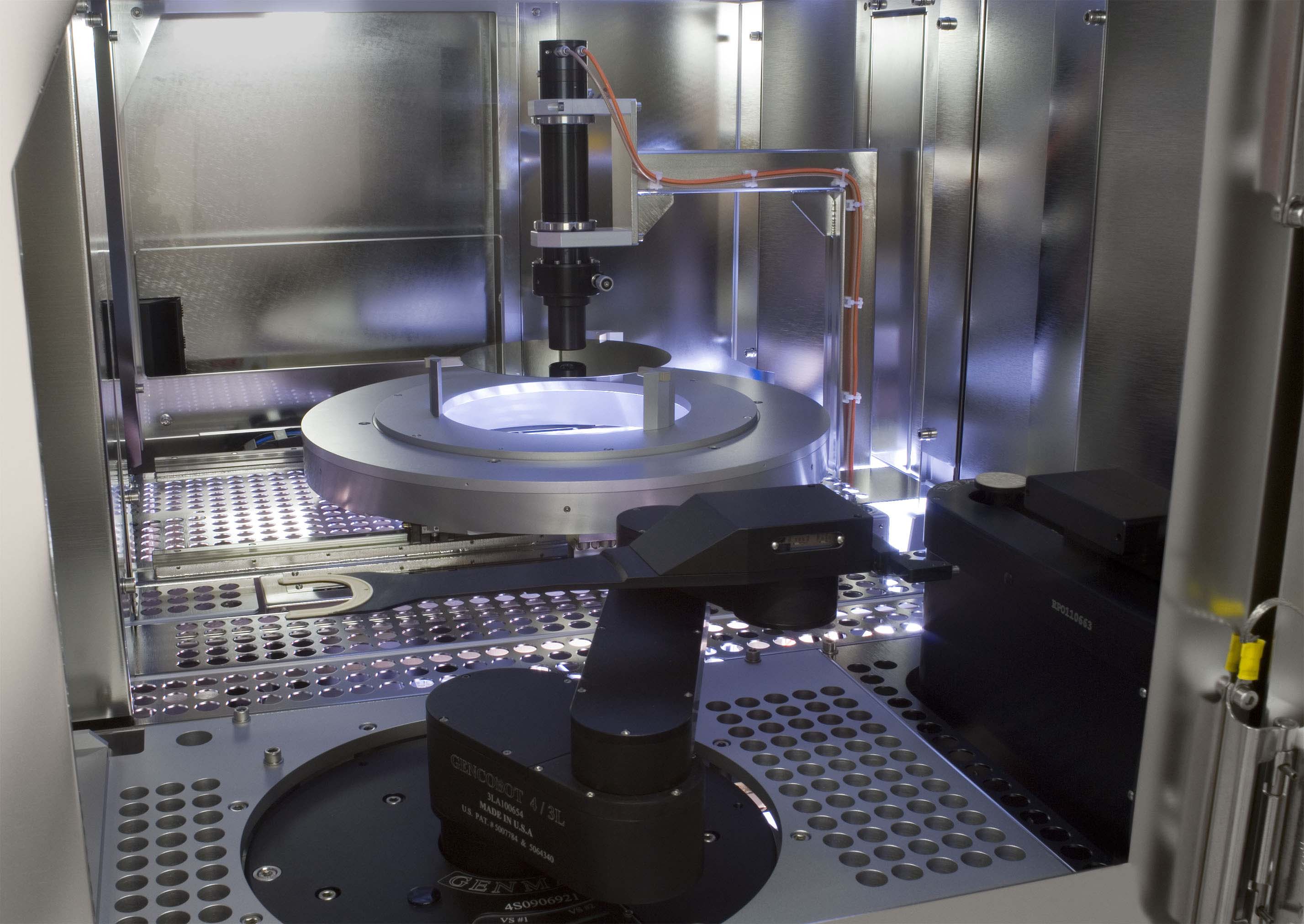
Advanced Chip Packaging plasma applications include plasma wafer cleaning for wafer level packaging, chip carrier plasma cleaning prior to wire bonding, encapsulation and Flip Chip under fill
A clean surface is the most important step you can do for making a quality bond, in addition to using a quality adhesive. The importance of having a clean surface
Gas plasma technology is commonly used to precision clean and activate, decontaminate surfaces, promote adhesion of functional bio-molecules and in conjunction with specific chemical vapors sterilize in-vivo and in-vitro medical
Gas Plasma is used widely throughout the world for a broad variety of industrial applications covering industries such as automotive, aerospace, batteries, electrical, food packaging, electronics, fuel cells
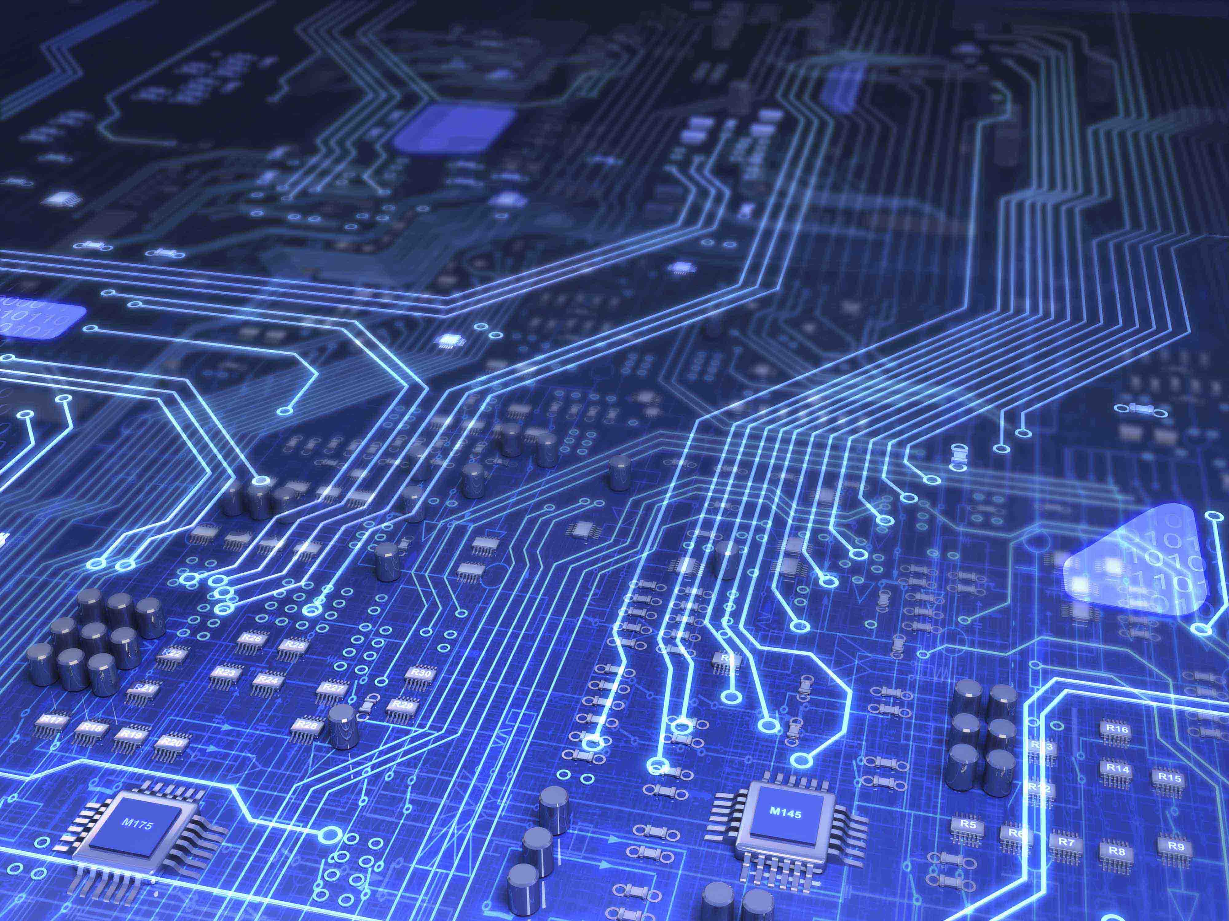
Plasma is used in the electronics industry for a wide variety of applications ranging from adhesion promotion of encapsulants and adhesives, to enhancing the release properties of optical disc master
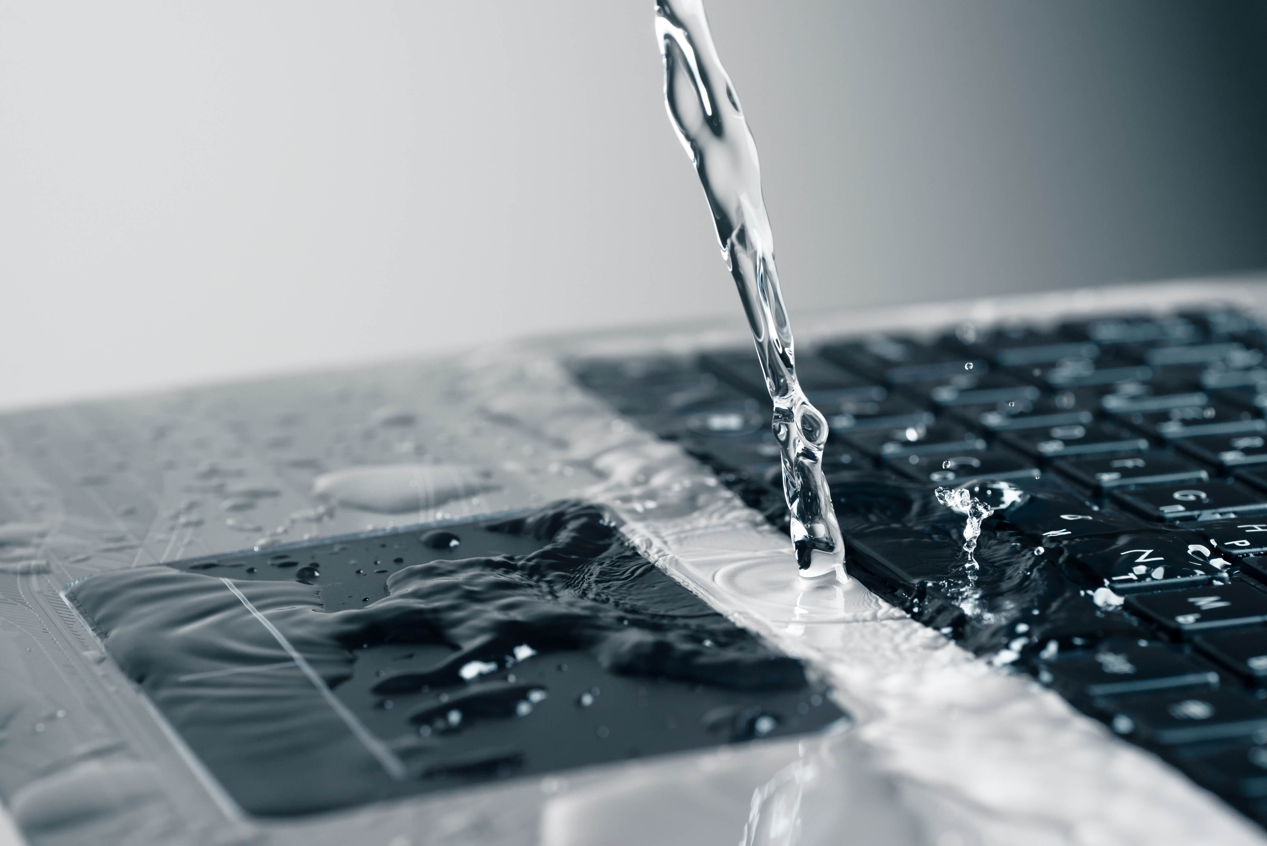
Plasma treated PCBs increases the surface energy of advanced materials, including fluoropolymer, providing excellent lamination, wettability and metalization through-holes without the use of wet chemicals.

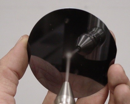
Wettability of hydrophobic materials by using a plasma process will help liquid material spread over the treated surface easily. The plasma process at PVA TePla America
Vacuum deposition of coatings at PVA TePla is utilized by a Plasma Enhanced Chemical Vapor Deposition (PECVD) process. This process is one of many types of deposition coating processes.

This technology provides significant environmental benefits and eliminates concerns such as wet chemistries, environmental permits, hazardous waste, bath degradation
Materials that need to have non stick properties is possible by using a low pressure plasma process. PVA TePla non stick coatings have low
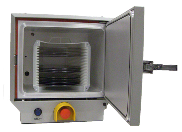
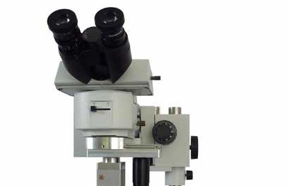
Plasma Cleaning is a dry, solvent free technology used to precision clean substrates at the molecular level. Precision cleaning is a requirement for a broad spectrum of industries with applications

The growth of thin films via chemical vapor deposition (CVD) is a powerful technique for bioassay, microarray, medical and microelectronic device (MEMS) fabrication. Chemical vapor deposition