
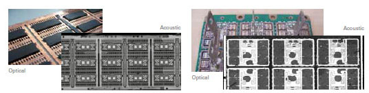
Scanning Acoustic Microscopes (SAM) are used for non-destructive failure analysis, research and development, quality control, and much more comprehensive testing for the semiconductor market. Delamination Detection is just one of the ways scanning acoustic microscopy is being used for testing in the semiconductor industry.
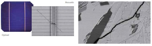
Scanning Acoustic Microscopes (SAM) have an advantage over optical microscopes. Such as examining a solar cell. A small internal crack was easily detected in the acoustic image wherein cracks are distinctively shown as clear black lines. Such a crack was not evident in the optical image even at higher magnification.
Scanning Acoustic Microscopes (SAM) are able to scan biological material such as bone structure and cells using frequencies between 80 Mhz and 1000 Mhz. This can produce quantitative estimates of sound velocity and acoustic attenuation inside the cells with a resolution of up to 1 μm. Acoustic micro images are one advantage of the PVA TePla America scanning acoutic microscope.