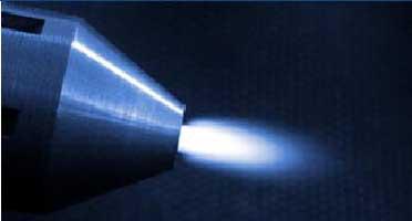
Plasma cleaning can also be applied to the packaging of Flat Panel Displays. For example, LCD or OLED terminal cleaning to remove organic contaminants from the bond fingers prior to connective bonding and conductive film adherence. Also glass activation by plasma prior to chip mounting (COG) is another important application. Because of the need for localized treatment these processes are best performed with PVA TePla’s atmospheric Plasma Pen. Due to the small size of the Plasma Pen nozzle, and the fact that it is attached to an umbilical, it can readily be integrated into a manufacturing line for either in-line or in-situ treatment of substrates.