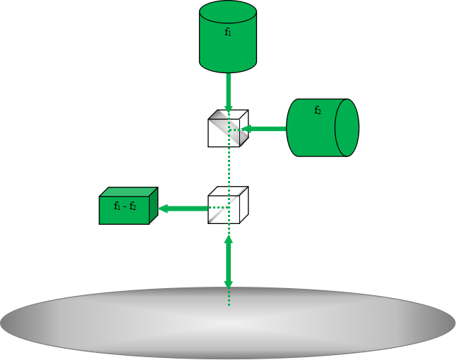
The Implant process is a very critical step within the integrated circuits manufacturing line. It defines important characteristics and properties of the devices-to-be by doping certain layers of the silicon substrate. Rework processes are very difficult and often impossible to apply. Therefore, the constant quality monitoring of the implant process is inevitable in order to maintain device yield. The result of the implant process can be measured and qualified on product wafers. The TWIN’s measurement range covers 10E10 to 5E16 dose levels at the implant energy level 1keV to 100 MeV.