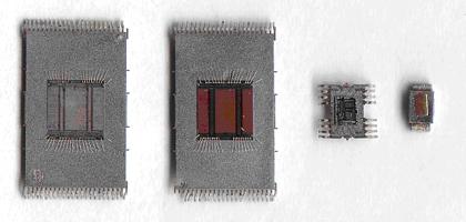
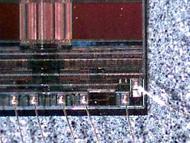
Decapsulation of packaged devices (such as integrated circuits (IC’s) and printed circuit boards (PCB’s)) exposes the internal components of the package. Opening devices by decapsulation allows inspection of the die, interconnects and other features typically examined during failure analysis. Device failure analysis often relies on the selective etching of polymer encapsulants without compromising the integrity of the wire bonds and device layers. This is achieved by using microwave plasma to cleanly remove encapsulant material. The etching properties of the plasma are highly selective leaving interconnects and bond pads unaffected by the plasma etching process. (Examples of decapsulated chips).