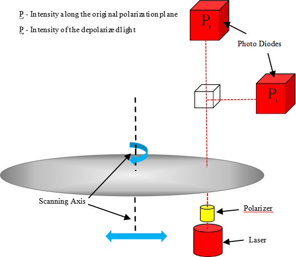
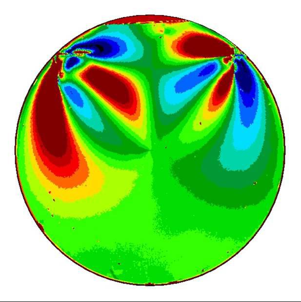
The introduction of 300mm wafers has imposed new, higher standard requirements on suppliers of bare wafers: By increasing diameter from 200 mm to 300mm, the wafer has more than doubled it’s surface area and weight, however the thickness has remained very much the same. This substantially increases the risk of breakage. 300mm wafers have high levels of internal mechanical tensions (stress), that significantly increase the breakage probability during the IC manufacturing process. This has obvious costly consequences. Therefore, the early detection of stressed wafers and prevention of breakage has gained more and more attention in recent years. Additionally, wafer stress also has a negative influence on Silicon crystal lattice characteristics. The SIRD is wafer level stress imaging system that makes significant contributions to cost reduction as well as yield improvement.