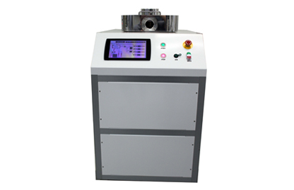
IoN 10Q Plasma System
The IoN 10Q Plasma System is a barrel plasma reactor designed for R&D and production applications. The technology is based…
Ion 40Q Plasma System
IoN 40Q Plasma System The Ion 40Q Plasma System is a barrel type plasma reactor. It is designed for batch…
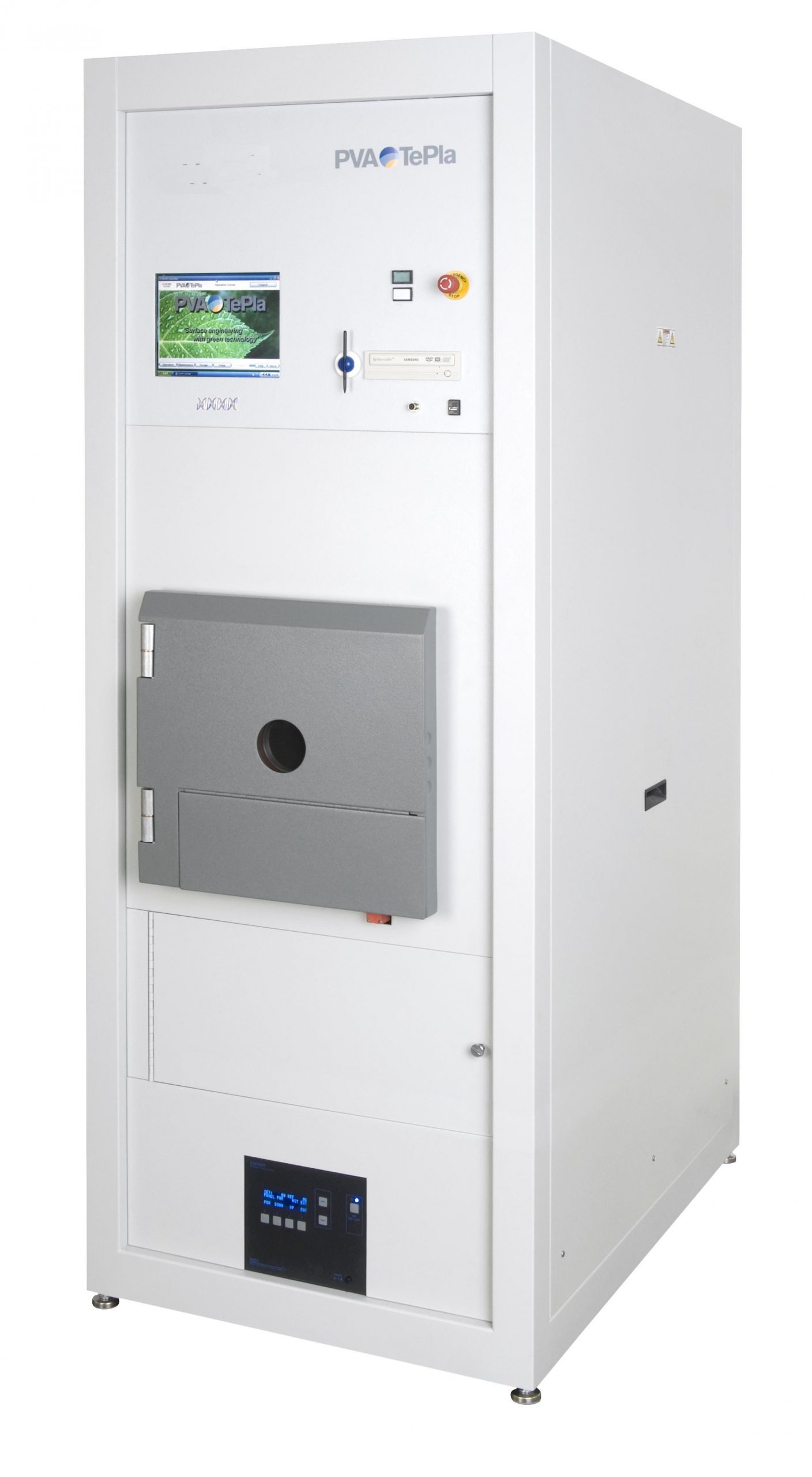
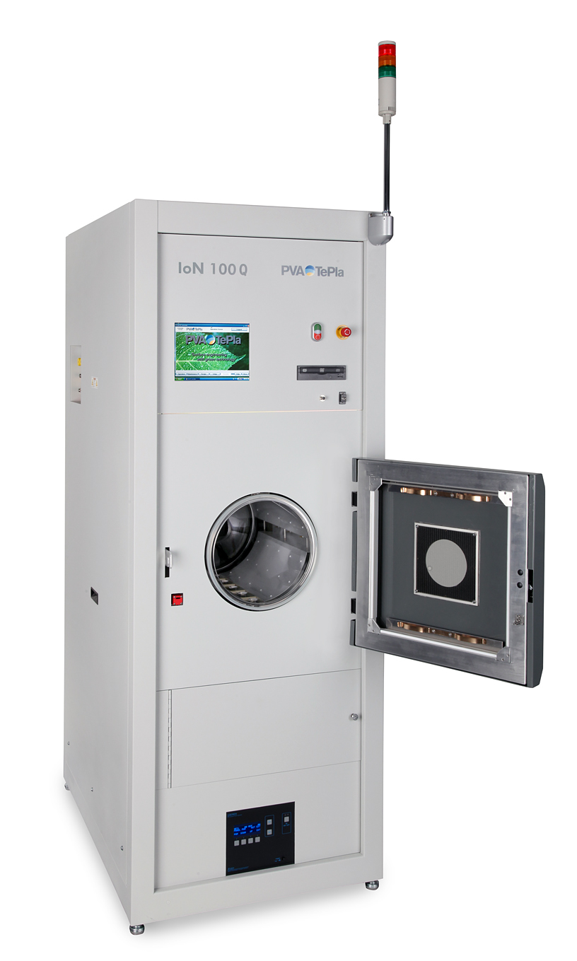
Photoresist Ashing IoN 100-40Q Plasma System
The Photoresist Ashing IoN 100-40Q Plasma System is a barrel plasma reactor designed for high volume production applications. The technology…
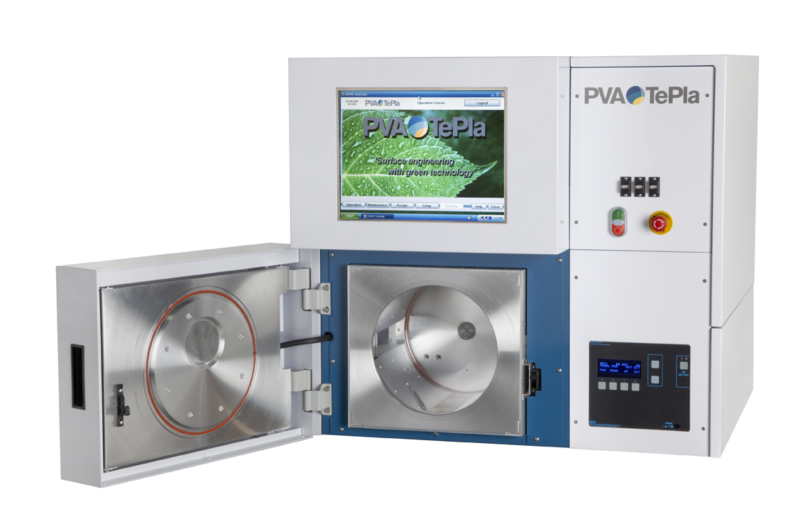
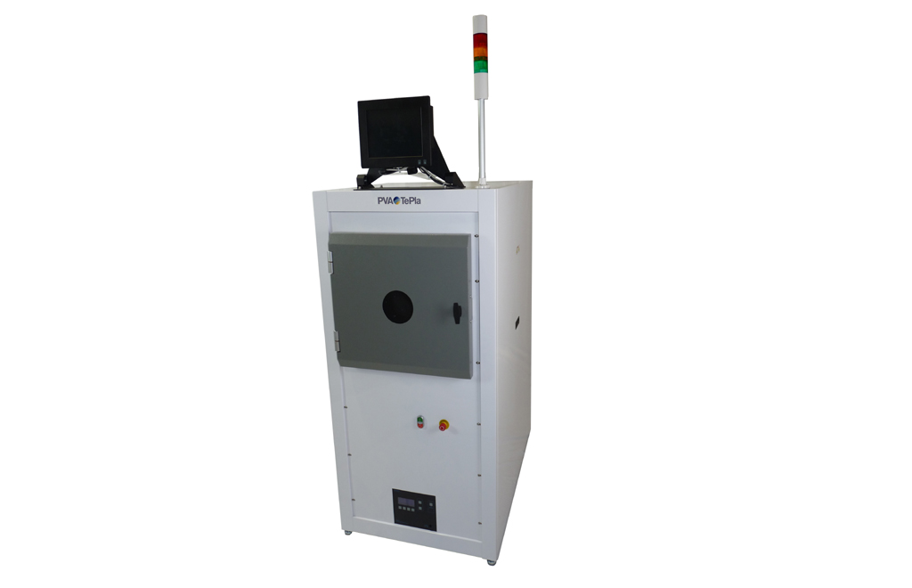
Photoresist Ashing IoN 100WB-40Q
The photoresist ashing IoN 100WB-40Q plasma system is designed for R&D and low volume production applications. The technology is based…
PHOTORESIST ASHING IoN 10V
SINGLE WAFER ASHING SYSTEM The Photoresist Ashing IoN 10V plasma system is a manual load single wafer RF plasma Ashing,…