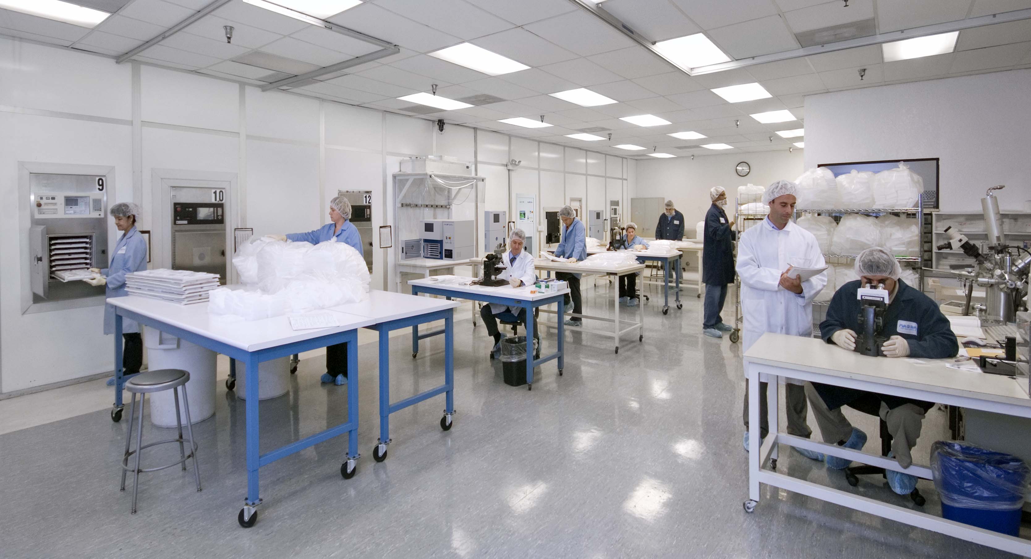
PVA TePla is one of the world’s leading system engineering companies. Its core competencies are in the fields of systems for hard-metal sintering and crystal growing as well as the use of plasma systems for surface activation, functionalization, coating, ultra-fine cleaning and etching.
Advanced Chip Packaging plasma applications include plasma wafer cleaning for wafer level packaging, chip carrier plasma cleaning prior to wire bonding, encapsulation and Flip Chip under fill
Improve adhesive bond properties of materials. Plasma is ideal for treating plastics, metals, ceramics, and glass prior to adhesive bonding. In each case, loose boundary films are removed and truly hyper-clean surfaces remain. For plastics,
Metallization of through-vias is often impeded by carbonaceous deposits formed during laser drilling. To remove these deposits from vias, the printed circuit boards are immersed into gas plasma

Plasma is used to promote the adhesion of anisotropic conductive film in flat panel display manufacture An LDI chip is attached to a tape-carrier package (TCP), and then connected to

Plasma desmear and etch-back by plasma is an established practice in the PCB industry. Drilling vias through multilayer PCB’s leaves residue, or smear, on the via walls.

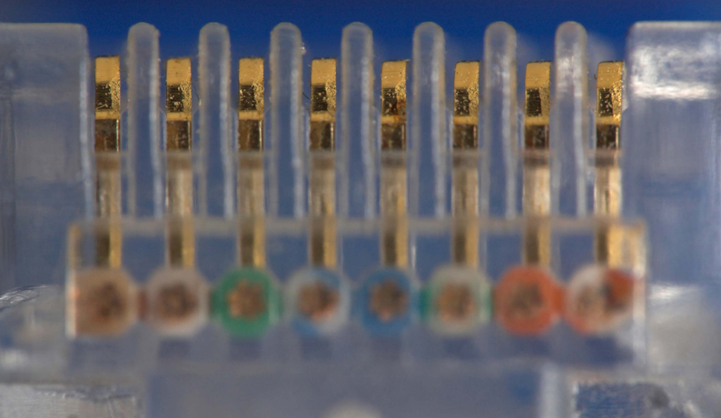
Electronic connectors and cable assemblies are used for communications and data transfer applications as well as for power connections. The insulative body around the contacts or feedthroughs often needs to
The global demand for graphite is surging and expected to continue for decades,driven by the broad use of graphite for
Ashing, in which the light–sensitive coating known as photoresist is removed and cleaned from an etchedwafer, is one of the
Traditional plate or shell and tube heat exchangers have long been used in processing industries. Today however, with many new
Joining dissimilar metals has tremendous potential for conformal cooling, but to successfully use diffusion bonding, a mold builder must understand
If you have any questions or suggestions, please don’t hesitate to get in touch with us directly. We will contact you.